

What Is Inside a Microchip?
- Starter
- Article
- Ages 10+
- 5 min read

Inside a microchip, transistors are formed on a semiconductor base, usually a silicon wafer, and joined into an electronic circuit. The circuit pattern is created on the wafer surface by lithography. Packaged on its own, the circuit and its semiconductor base become a chip for use in devices.
Contents
What you will learn
- Name the semiconductor base, the transistors and the integrated circuit inside a chip.
- Retell the four steps that build a circuit on a wafer and what each one does.
- Distinguish a wafer from a packaged chip.
Before you start
This article reads best after “What Is a Microchip?”, but each term is explained as it appears.
What base is a chip built on?
A chip’s circuit sits on a wafer, a thin piece of semiconductor material that serves as the base for building many integrated circuits at once. Silicon wafers are the most common. Wafers can also be made from gallium arsenide, silicon carbide or germanium.
The process begins by slicing semiconductor material into a thin segment. The segment is then ground and polished by a series of specialised machines. After these operations, the base is ready to receive a circuit.
One wafer carries many circuits, so it differs from a chip. In NIST’s example, the surface of a silicon wafer contains thousands of integrated circuits. The wafer is the shared base, and each circuit is only a small part of it.
How is the circuit formed on the base?
An integrated circuit combines many transistors into a small circuit on a chip. Each transistor is a semiconductor switch that turns on or off with voltage. To place enough transistors in the right positions, the circuit is built on the wafer surface in four steps.
- Oxidation. The wafer is cleaned first. For silicon wafers, this step can also involve heating and exposure to pure oxygen.
- Masking. Photomasks, very precise stencils, create patterns on the wafer. Each mask helps define the circuit.
- Etching. Unneeded material is removed from the wafer, leaving the intended shape.
- Doping. Impurities are added to the crystal structure to change its electrical properties.
Lithography is the general name for etching into or building onto a wafer surface to produce integrated-circuit patterns. Each step answers a different question: where the pattern lies, which material stays, and what electrical properties each region has.
What does the complete chip include?
A chip is a self-contained piece that includes the semiconductor surface and the integrated circuit, packaged for use in electronics. From outside, you see only the package. The circuit and its base sit within, which is why the cutaway illustration opens them up.
The whole chain from bare wafer to working chip takes place in a fab, the industrial facility built for the job.
Real-world example
Suppose you present a chip model to a class. Point to the large sheet and call it a wafer, because it is the base for many integrated circuits. Point to one small circuit region on it and say the transistors are combined there. Point to the packaged component and call it a chip.
Then retell the journey of the base. It is sliced thin, ground and polished. Masks create the pattern, etching removes unneeded material, and doping adjusts the electrical properties. Finally the circuit is packaged.
If the model swaps the labels and your story stays the same, you are ignoring how base, circuit and component relate. A correct explanation says which part is the base, which is the circuit and which is the ready-to-use component.
Common misunderstandings
A wafer is not yet a chip. The wafer is a base holding many integrated circuits, while a chip is a component packaged on its own.
An enlarged illustration shows how the parts relate. The real size of each transistor cannot be read from it.
The four steps above are how the source describes building an integrated circuit. They are not instructions for making a chip yourself.
Frequently asked questions
What is a wafer made from?
A wafer is a thin sheet of semiconductor material. Silicon is the most common, and others include gallium arsenide, silicon carbide and germanium.
What is lithography for?
Lithography produces integrated-circuit patterns on a wafer surface, using masks and the removal of unneeded material.
At which step does doping happen?
It is the last of the four steps the source describes. Impurities are added to the crystal structure to change its electrical properties.
Summary
Terms in this article
English and Vietnamese terms, with the meanings used here. Hover, tap or Tab to a term with a dotted underline for an explanation as you read.
- wafer
- A thin semiconductor sheet providing a base for multiple integrated circuits.
- lithographyquang khắc
- A process producing circuit patterns on a wafer surface.
- integrated circuitvi mạch
- A small circuit combining many transistors on a chip.
- chip
- A self-contained piece with a semiconductor surface and integrated circuit, packaged for use in electronics.
- dopingpha tạp
- Adding impurities to a semiconductor's crystal structure to change its electrical properties.
- fab
- An industrial facility where raw silicon wafers become fully working chips.
This article is not marked as viewed
Spotted something wrong or unsafe?
Tell the administrator by email. The message already has the article title and address.
More in this topic
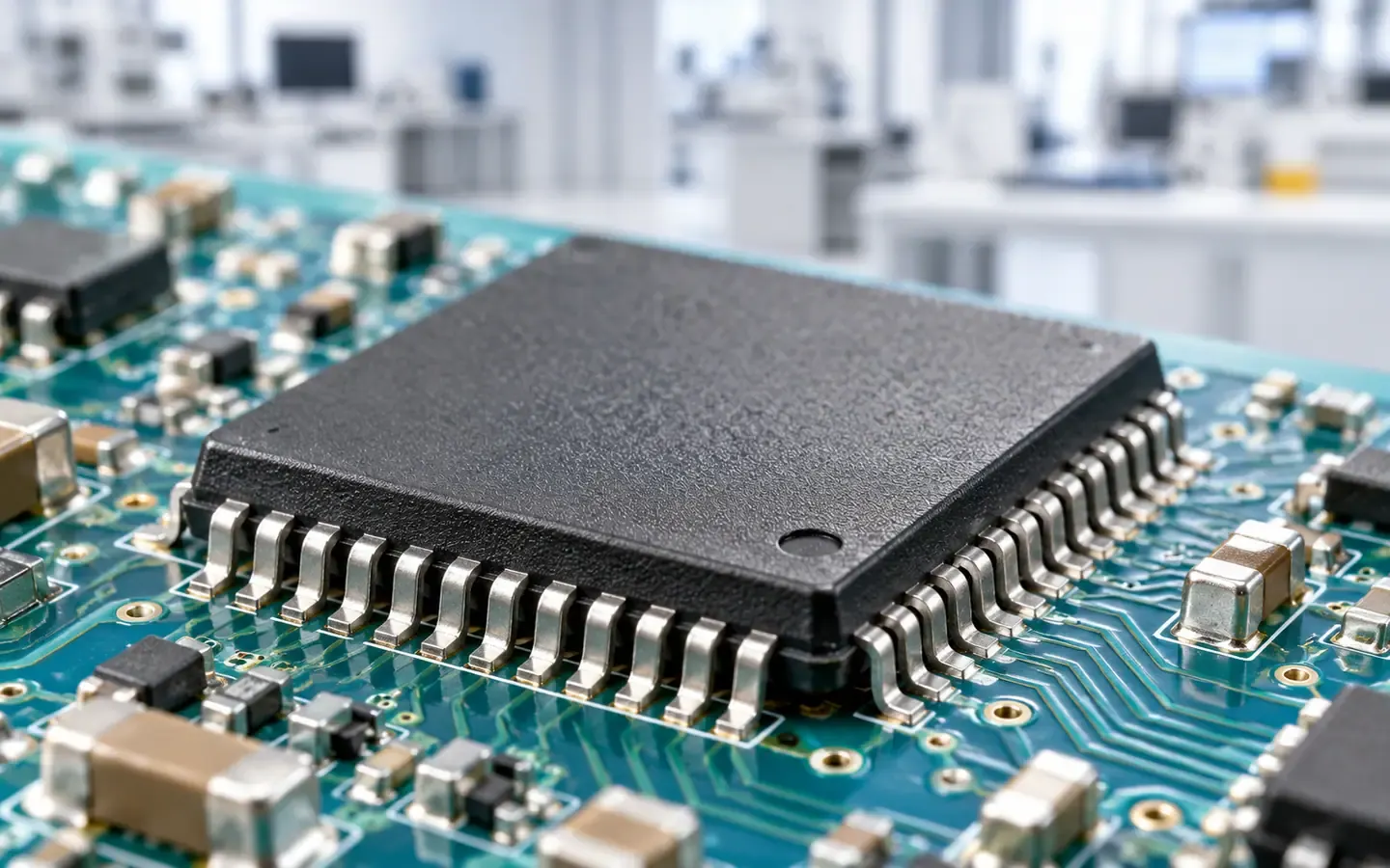 Starter
What Is a Microchip?
Understand microchips, transistors and chip packages through a phone example, and distinguish a semiconductor material from a finished circuit.
5 min read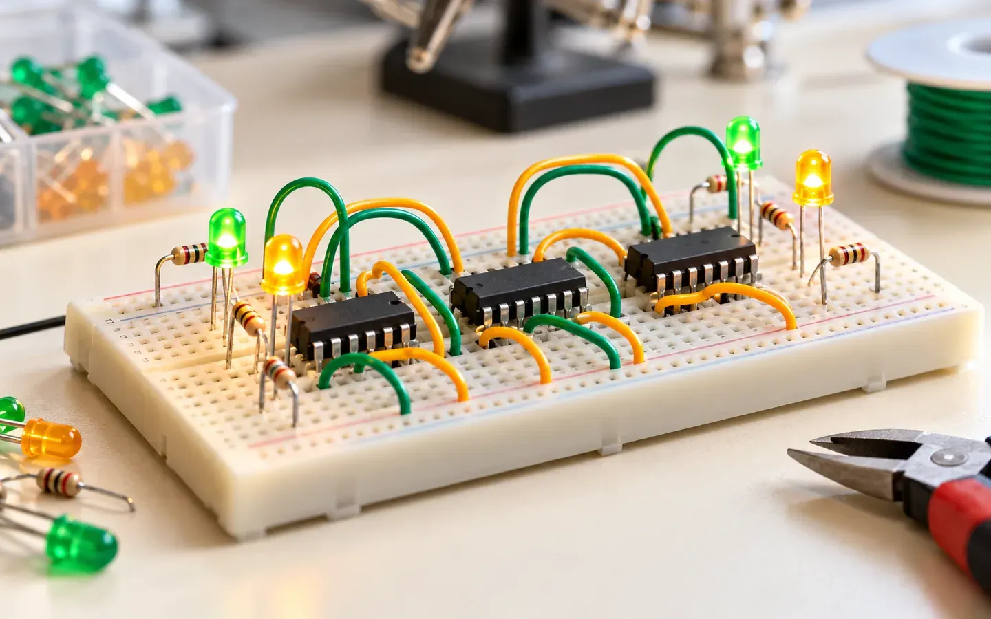 Basic
How Do Logic Gates Combine to Process Signals?
Follow signals through AND, OR and NOT gates using truth tables and a worked light-control example to understand combined logic.
5 min read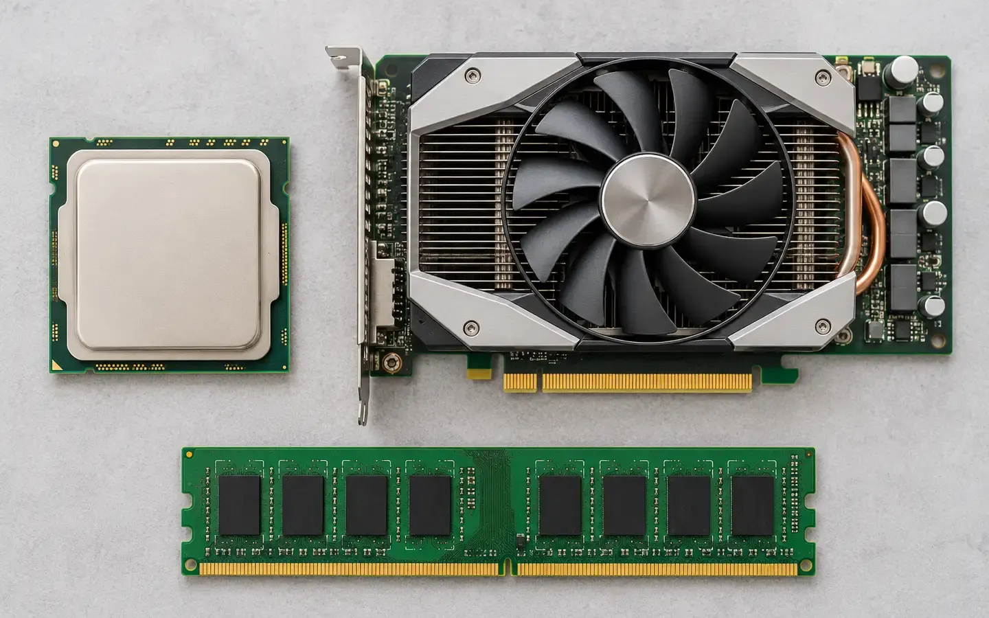 Basic
How Do CPU, GPU and Memory Chips Differ?
Compare CPU, GPU and memory by role, processing style and cooperation in an application, rather than treating them as interchangeable speed upgrades.
3 min read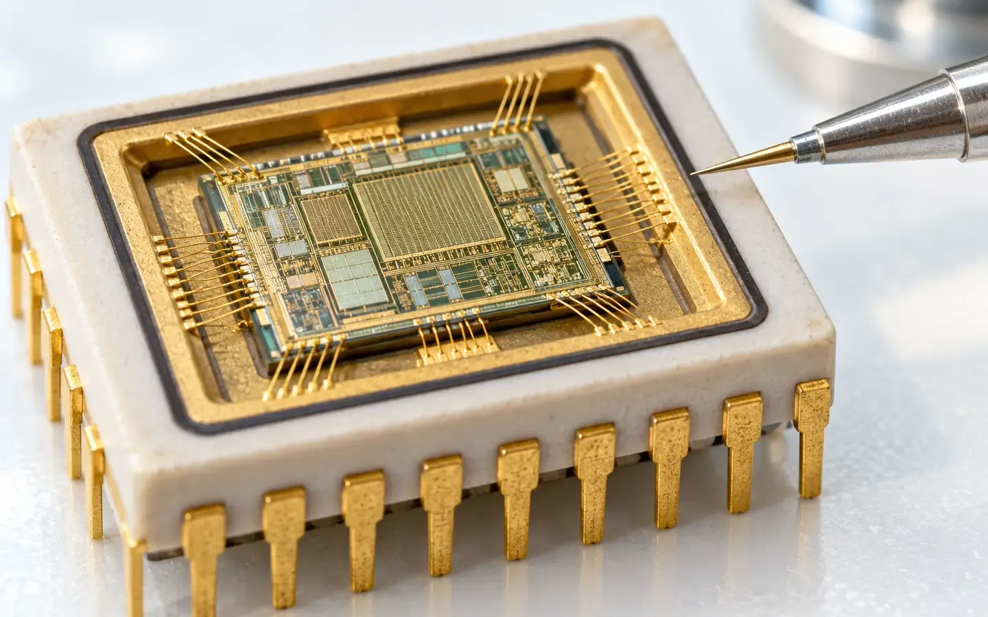 Intermediate
How Does a Microchip Process Instructions?
Follow an instruction through fetch, decode, operand reading, execution and writeback; distinguish a CPU model from all chips and from clock cycles.
3 min read


Sources
These sources are written for older readers. If they feel hard, read them with an adult.
- Semiconductor Glossary(opens in a new tab)
NISTTier A: government, standards or research bodiesRead on October 31, 2026
- What is a semiconductor?(opens in a new tab)
IBMTier B: vendor documentationRead on October 31, 2026