

How Does a P-N Junction Work?
- Basic
- Article
- Ages 12+
- 3 min read

When p-type and n-type semiconductor regions meet, carriers diffuse across their boundary. Fixed charges left behind form an electric field and a region depleted of mobile carriers. An applied voltage changes this barrier, making current depend on bias.
Contents
What you will learn
- Explain how a depletion region forms.
- Compare forward and reverse bias on one junction.
- Distinguish equilibrium from an absence of carrier motion.
Before you start
Read the linked prerequisite first. This article explains principles and does not require assembling or opening equipment.
From diffusion to an electrical barrier
The n side has many electrons and the p side many holes. Concentration differences drive electrons toward p and holes toward n. As carriers move, charges at dopant sites are exposed.
The n side leaves positive ions and the p side negative ions. These charges are fixed in the lattice, with the field directed from n toward p. They create an electric field across the boundary, leaving the nearby region depleted of mobile carriers. A depletion region is not an empty gap without atoms; it lacks free carriers.
- Depletion region
- Semiconductor on both sides
- Left — holes in the p region
- Right — electrons in the n region
What does an applied voltage change?
Forward bias reduces the net field at the junction, making carrier diffusion across the barrier easier and increasing diffusion current. In this diode model, p is positive relative to n.
Reverse bias increases the field and reduces diffusion current. “Reduced” does not mean every current becomes zero: the source distinguishes diffusion current from drift current.
Equilibrium does not mean every carrier stops
Without an external input such as light or applied voltage, component currents balance and net current is zero. Opposing contributions that cancel are a better picture than frozen carriers.
Diffusion, the field and external conditions together explain junction behaviour. Simply naming positive and negative sides without the barrier mechanism cannot explain forward versus reverse bias.
A worked example
Follow one illustrative p-n junction through three states. This is a model interpretation, not a measurement on a real diode. State one: the p and n regions have just been joined. Electrons diffuse from the n side toward p and holes diffuse from p toward n, leaving fixed positive ions on the n side and fixed negative ions on the p side. These ions set up a field directed from n toward p, so the region near the junction is depleted of mobile carriers.
State two: an external voltage is applied with the p side positive relative to n (forward bias). The net field at the junction falls, carriers diffuse across more easily and the diffusion current increases. State three: reverse the voltage (reverse bias). The field grows and diffusion current falls, although the source does not say all current becomes zero. With no external voltage, the component currents balance and the net current is zero; ask yourself why that does not mean the carriers are standing still.
Frequently asked questions
Is the depletion region empty?
No. The lattice remains; mobile carriers are depleted.
Does reverse bias mean current is always zero?
No. Reducing diffusion current does not eliminate every current contribution.
Summary
- Diffusion exposes fixed charges and forms a field.
- Applied voltage changes the carrier barrier.
- Compare biases through fields and currents.
Terms in this article
English and Vietnamese terms, with the meanings used here. Hover, tap or Tab to a term with a dotted underline for an explanation as you read.
- depletion regionvùng nghèo
- A region near a junction depleted of mobile carriers.
This article is not marked as viewed
Spotted something wrong or unsafe?
Tell the administrator by email. The message already has the article title and address.
More in this topic
 Basic
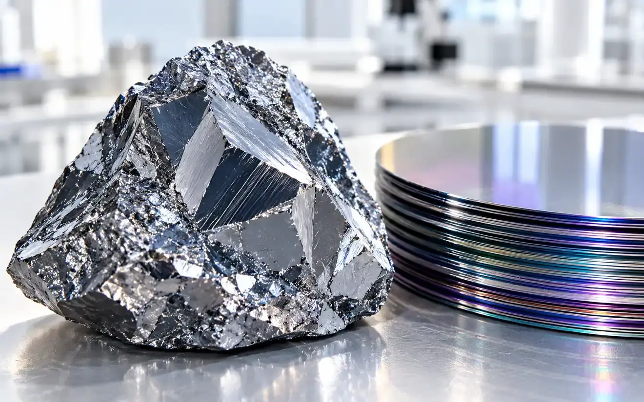
Why Is Silicon Used in Electronic Components?
Understand silicon’s use in electronics through its availability, adjustable electrical properties and suitability for making wafers.
5 min read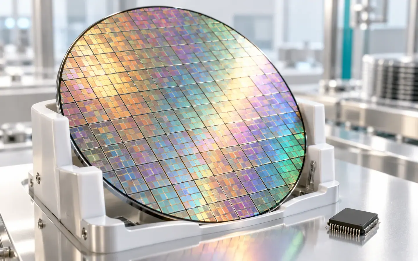 Starter
What Are Semiconductors?
Learn about semiconductor materials, controlled conduction and doping, and distinguish the material from a transistor or a packaged chip.
5 min read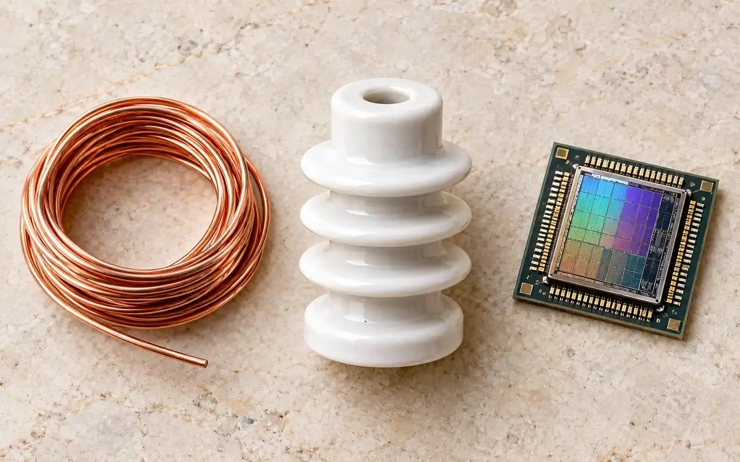 Starter
How Do Conductors, Insulators, and Semiconductors Differ?
Compare conduction and the roles of conductors, insulators and semiconductors, and see why electronic components use different materials.
5 min read Intermediate
How Does Doping Change a Semiconductor?
Explain how intentional doping changes semiconductor carriers; compare n-type and p-type material and distinguish a hole from an empty atomic site.
3 min read


Sources
These sources are written for older readers. If they feel hard, read them with an adult.
- Formation of a PN-Junction(opens in a new tab)
PVEducationTier C: other sourcesRead on October 31, 2026
- Bias of PN Junctions(opens in a new tab)
PVEducationTier C: other sourcesRead on October 31, 2026