

Why Is Silicon Used in Electronic Components?
- Basic
- Article
- Ages 12+
- 5 min read

Silicon is used widely in electronics because it is a semiconductor whose conduction can be adjusted, it is abundant, and it is available as wafers for making chips. It occurs in sand, but must be refined before it becomes crystalline silicon that conducts. That makes silicon both useful and inexpensive.
Contents
What you will learn
- State the properties that make a semiconductor suitable for electronics.
- Explain the path from sand to usable silicon crystal.
- Compare silicon with other semiconductor materials and recognise its limits.
Before you start
This article reads best after the one on semiconductors, but each term is explained as it appears.
What does electronics need from a semiconductor?
Electronics needs a material whose conduction we can control. A semiconductor provides it. The “semi” means its electrical conductivity is less than that of a metal but more than that of an insulator.
Most semiconductors are made of crystals, typically silicon. Common conducting elements have a single electron in their outermost shell, while semiconductors have four. This, with other factors, makes silicon crystal suited to controlling current.
Control comes from doping: deliberately introducing impurity atoms into the crystal to change its electrical properties, making the material more or less conductive. Silicon allows this adjustment, so components made from it can be switched on or off as the designer intends.
Why is silicon easy to obtain and cheap?
Silicon is an abundant element found in sand, so the raw material is inexpensive. Sand cannot be used as it is, though. Silicon has to go through a chemical refining process before it becomes crystalline silicon that conducts electricity.
This matters for comparison. A material that is electrically excellent but scarce or expensive is hard to use at scale. For silicon, a common raw material found in sand helps keep the cost low.
How do crystal, wafer and product connect?
Crystalline silicon is cut into thin sheets called wafers. Silicon wafers are the most common wafers for making integrated circuits. The same principle is used for solar panels: blocks of crystalline silicon are cut into very thin wafers and processed into photovoltaic cells.
So one material serves two kinds of product. About 95% of solar panels on the market use either monocrystalline or polycrystalline silicon. Silicon is also the main semiconductor in most electronics.
Silicon is not the only choice. Wafers can also be made from gallium arsenide, silicon carbide or germanium. Radio-frequency chips combine gallium arsenide, gallium nitride and silicon to work at higher frequencies. Silicon solar cells have a theoretical maximum efficiency of about 32%, a trade-off of the material.
Real-world example
Compare a rooftop solar panel with the chip in a phone. Both start from sand refined into silicon crystal. Both use wafers cut thin from the crystal.
The difference lies in the processing that follows. A solar wafer is processed into a photovoltaic cell, while a chip wafer has circuits formed on it. One material, two uses, thanks to different processing.
Common misunderstandings
Silicon is not sand. Sand contains silicon, but it needs chemical refining before it becomes crystal that can conduct.
Silicon is not the only semiconductor. Germanium, gallium arsenide, gallium nitride and silicon carbide are also used, depending on purpose.
A wafer is a form of the material, not yet a product. The same kind of wafer can become a chip or a solar cell.
Frequently asked questions
Is silicon really found in sand?
Yes. Silicon occurs in sand, but it needs chemical refining before it becomes usable crystalline silicon.
Why do chips use silicon wafers?
Silicon wafers are the most common. Silicon is a typical semiconductor whose electrical properties can be adjusted by doping.
Does silicon have limits?
Yes. For solar cells, the theoretical maximum efficiency of a silicon cell is about 32%. Some radio-frequency circuits also need gallium arsenide or gallium nitride.
Summary
- Silicon is a semiconductor whose conduction can be adjusted by doping.
- It is abundant in sand but must be refined into crystal.
- Silicon wafers serve both chips and solar panels, although other materials suit particular needs.
Terms in this article
English and Vietnamese terms, with the meanings used here. Hover, tap or Tab to a term with a dotted underline for an explanation as you read.
- silicon
- A common semiconductor material used in electronics and photovoltaic cells.
- wafer
- A thin semiconductor sheet used in device manufacturing.
- dopingpha tạp
- Deliberately introducing impurity atoms into a crystal to change its electrical properties.
- semiconductorbán dẫn
- A material that conducts or resists current depending on conditions.
This article is not marked as viewed
Spotted something wrong or unsafe?
Tell the administrator by email. The message already has the article title and address.
More in this topic
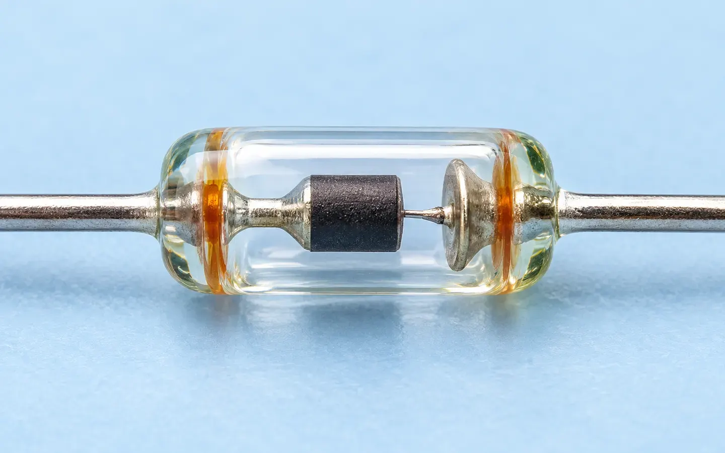 Basic
How Does a P-N Junction Work?
Understand diffusion, depletion and the p-n junction field; compare forward and reverse bias through carrier motion without building a circuit.
3 min read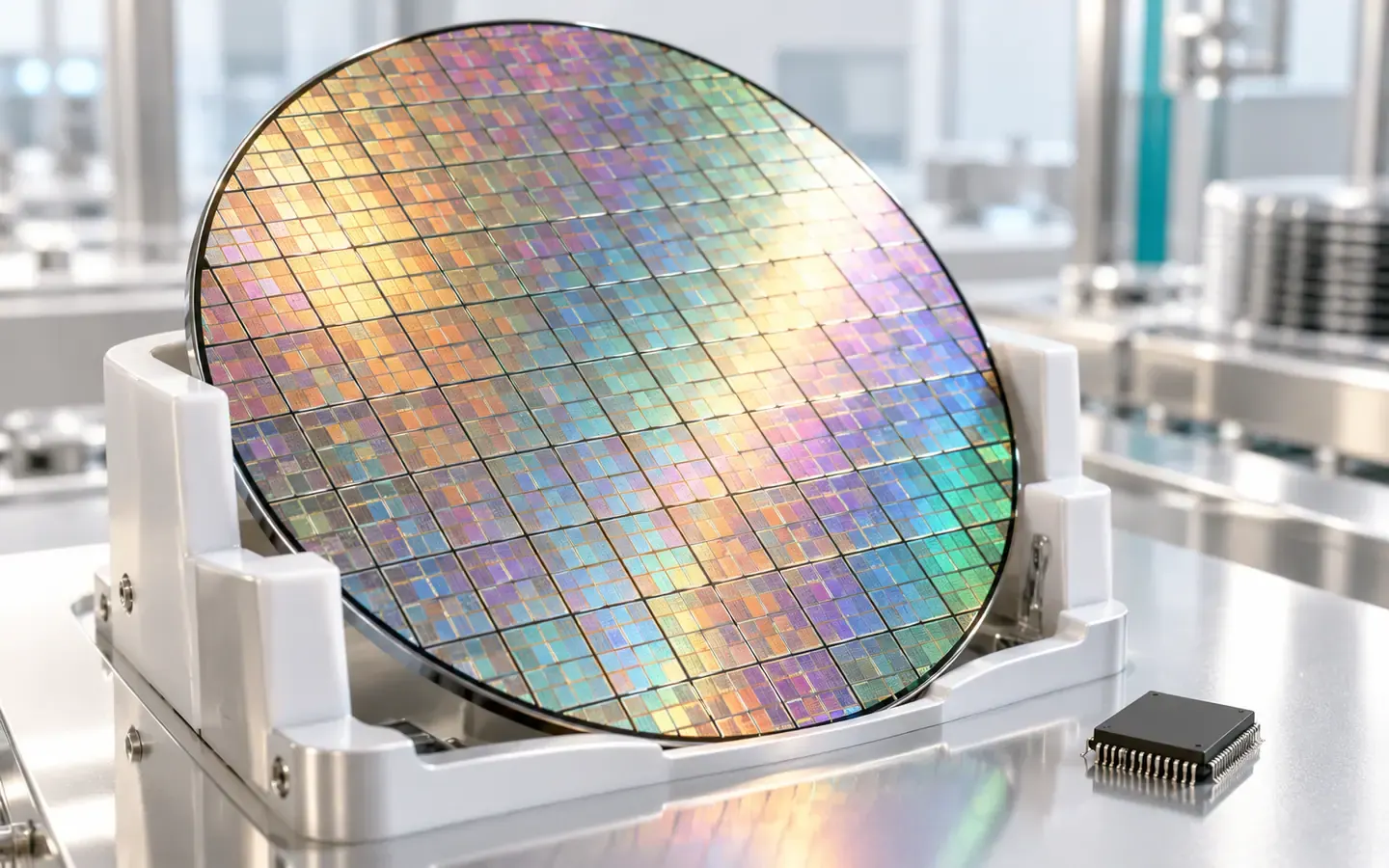 Starter
What Are Semiconductors?
Learn about semiconductor materials, controlled conduction and doping, and distinguish the material from a transistor or a packaged chip.
5 min read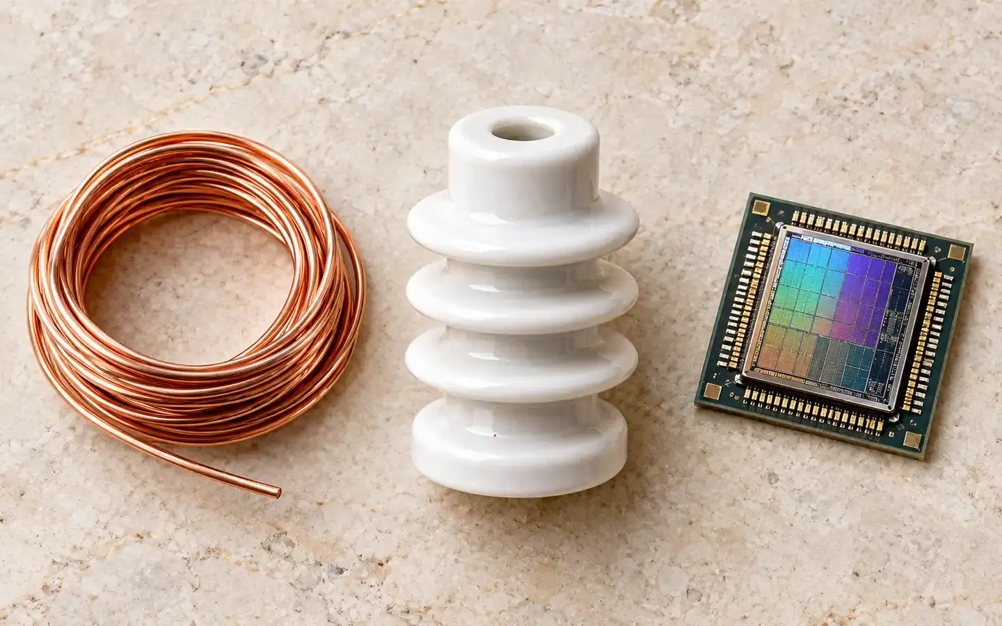 Starter
How Do Conductors, Insulators, and Semiconductors Differ?
Compare conduction and the roles of conductors, insulators and semiconductors, and see why electronic components use different materials.
5 min read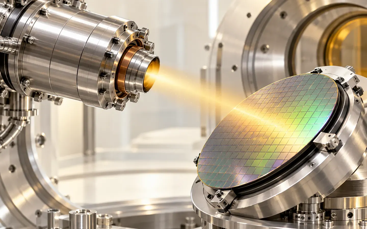 Intermediate
How Does Doping Change a Semiconductor?
Explain how intentional doping changes semiconductor carriers; compare n-type and p-type material and distinguish a hole from an empty atomic site.
3 min read


Sources
These sources are written for older readers. If they feel hard, read them with an adult.
- What is a semiconductor?(opens in a new tab)
IBMTier B: vendor documentationRead on October 31, 2026
- PV Cells 101: A Primer on the Solar Photovoltaic Cell(opens in a new tab)
US Department of EnergyTier A: government, standards or research bodiesRead on October 31, 2026